Q. What are the symptoms of target overheating?
A. Dramatic, immediate changes in voltage and/or current are indications of target overheating. Check for:- Inadequate water flow
- Inlet water temperature not per specification
- Poor target bonding or target clamping
- Higher than permissible power density per duty cycle
- Magnet module strength degradation
Q. Why won't the plasma ignite?
A. Verify the following: - All power supply/system interlocks (water/pressure/flow) are satisfied
- Argon gas pressure at target surface is sufficient
- Power supply is properly connected to the cathode and chamber
- Chamber pressure is not too high
- Water leaks are not causing shorting (verify with an ohm meter)
- No shorts between cathode and the ground shield (anode) caused by whisker growth, flaking or debris (verify with an ohm meter)
- Insulator surfaces (not outside surfaces of screw insulators) are not coated or conductive (verify with an ohm meter)
- Magnet module has not been overheated or weakened (verify with a gaussmeter against the magnetic field profile shipped with sputtering source)
- Excessively thick magnetic targets are not being used
- Target material is electrically conductive when using a DC power supply
- When using RF power - verify that the forward and reflected power is being displayed and that the reflected power is close to zero.
Q. Weak Plasma Discharge - Low Deposition Rates
A. Verify: - Check for electrical leakage across insulators using an ohm meter
- Power is being transmitted through the cooling water lines - check for proper resistivity using an ohm meter with the water flowing through the water lines
- Weak magnet module - verify against supplied profile. Are the magnets being sufficiently cooled?
- Poor or no ground connection
- Suspect a weakened magnet module when target utilization degrades over time for the same thickness and type of material used in an unchanged process
environment. The erosion groove profile usually begins to become more pinched and wobbly in this circumstance. This will correlate to the fact that the
power supply voltage must be increased to maintain the same power output. A sure indication that the magnet module must be replaced is when new targets
cannot sustain the desired applied power level - Insulating film build-up on target surface (DC or pulsed DC power supply). Severely contaminated targets can take hours or even days to clean. Severe
arcing usually is symptomatic when attempting to raise the target voltage. - Is the pressure at the target surface adequate for efficient magnetron sputtering?
Q. Plasma extinguishes or is intermittent
A. Check for: - Insufficient pressure - check mass flow controllers, throttle valve and gas supply
- Whisker growth or debris causing shorting between the cathode and ground shield (anode)
- "Disappearing Anode." This occurs when all available ground return paths have been coated with an insulating film. All chamber surfaces at ground potential and the sputter source anode surfaces must be removed and cleaned.
Q. Milky Films
A. Can be caused by: - Air leak in system
- Water leak in system
- Leak in argon or reactive gas lines
Q. Galvanic corrosion of parts exposed to cooling water 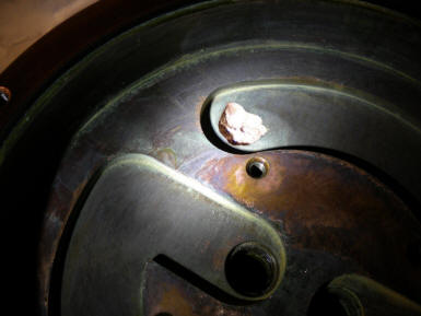
A. Check for: - Low water resistivity - check for proper resistivity
- Additives in proprietary solutions used in closed-loop water recirculation or house water are inappropriate
- De-ionized water is being used - immediately eliminate it's use
- Materials other than copper, brass, stainless steel, PTFE and appropriate plastics are contained in closed-loop or house water system - immediately eliminate their use.
Galvanic corrosion in copper cathode body caused by ion
exchange due to inappropriate materials in cooling system
Q. Cannot run DC power supply at rated power levels
A. This is a particular problem when newer model pulsed DC power supplies with low upper voltage limits are used at low pressures (less than 1 mTorr) in
combination with sputtering sources having relatively low target surface areas (higher impedance compared to larger, lower impedance targets). Ensure that
the power supply purchased is a "high Z" (widest voltage range with highest possible output voltage) version to prevent power limits at low pressures. Increasing the chamber process pressure will lower the overall impedance, allowing higher power levels. In some instances, it may be useful to double the
effective surface area by driving two sputtering sources of the same size with a single power supply (decreases the impedance at the same operating
pressure). Both sputtering sources must be in the same process chamber and exposed to the same process conditions. - Low water resistivity
- Additives in proprietary solutions used in closed loop water recirculators or house water are inappropriate
- De-ionized water is being used - Immediately eliminate it's use.
- Source is operating at low pressure (typically less than 1 mTorr) and power supply has a low upper voltage limir. This is typical of newer pulsed DC power supplies
- High atomic weight materials like Au (gold) require several hundred volts more output from the power supply at equivalent pressures and operating conditions compared to most other commonly sputtered materials. In practice, this often means that the total power that can be applied to the target is limited by the upper voltage limit of the power supply. Here are some suggestions to alleviae this problem:
- Select the highest possible voltage tap on the power supply transformer
- Raise the operating pressure to suppress the voltage required. Be aware that increasing the pressure to too high a level can actually reduce the effective sputtering rate due to gas scattering. This pressure will vary by circumstancess and system, but will occur in the region of 10 mTorr
- Change the sputtering gas from argon to kryton, xenon or an argon/kryton argon/kryton gas mixture. It's desirable to match the atomic weight of the material being sputtered as closely as possible to that of the sputtering gas to achieve the best sputter yield/rate. The atomic weight of argon is nominally 40, compared to nominal 84 for krypton and 131 for xenon. The atomic weight of gold is nominally 196
Here is a summary of the sputter yields for various gases @ 600 eV ion energy:
He - .08
Ne - 1.15
Ar - 2.75
Kr - 3.40
Ze - 3.40
Increasing the ion energy to 1000eV for Ar results in a sputter yield of 3.6. We have no data available for the sputter yields of the other gases at this higher energy level, but it is reasonable to assume the yield would be roughly equivalently increased.
The short summary - use power supplies with an upper voltage limit of at least 1000 volts and consider the use of more expensive gases and gas mixtures (compared to pure argon) to maximize the total power that can be applied to a high molecular weight material like gold. Consider running at higher pressures than you would normally.
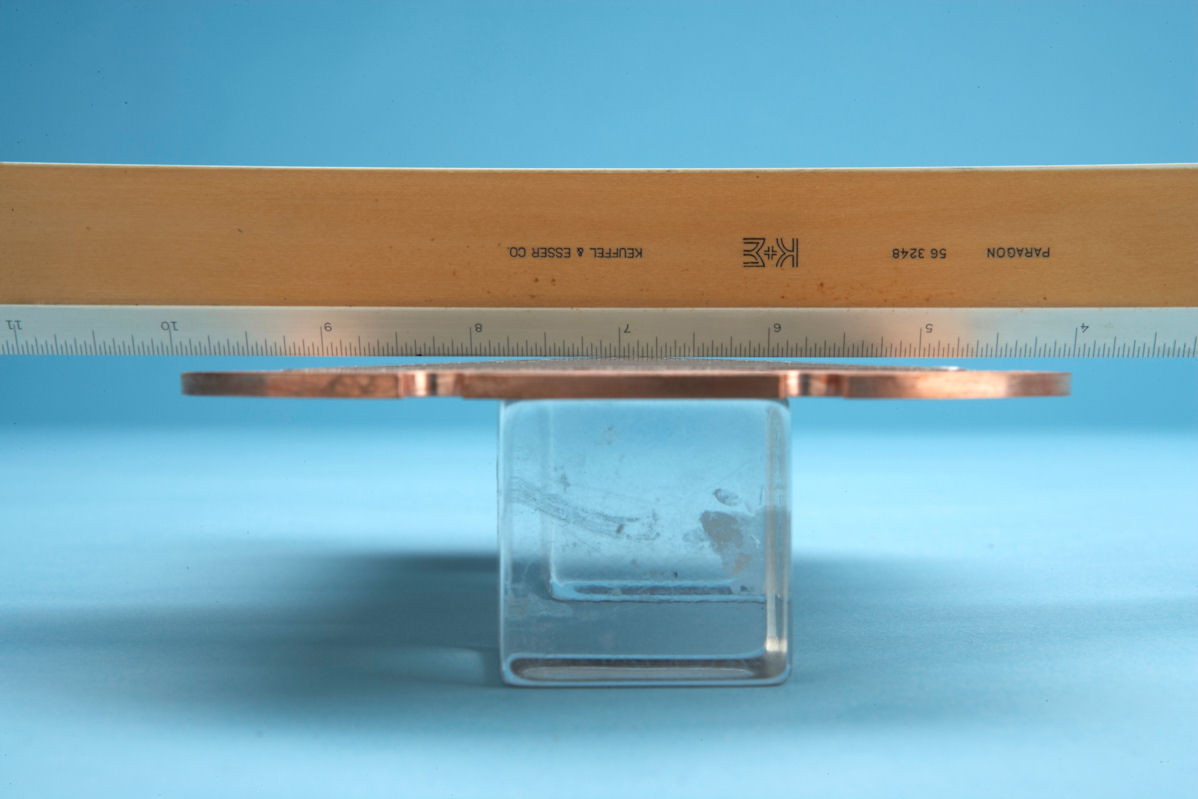
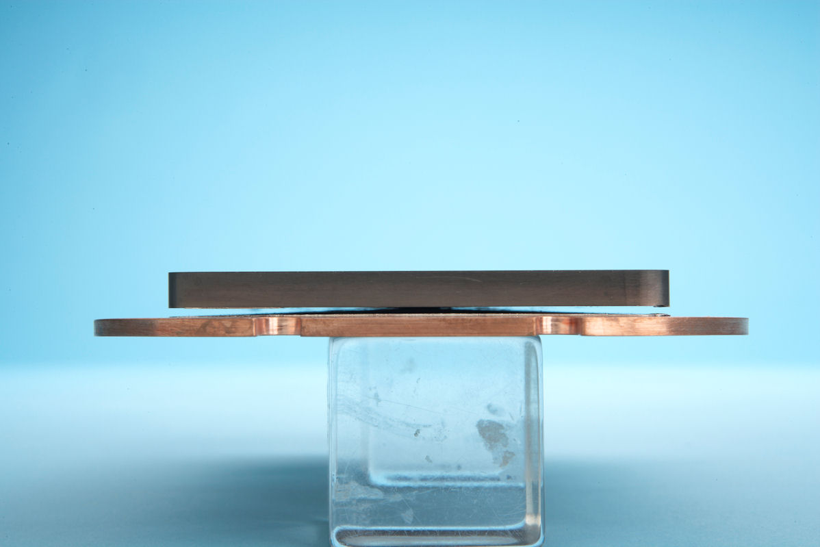
Q. Excessive Target Backing Plate Deflection
A. Possible causes: 
Backing plate is too thin for the material it is made out of and is not structurally strong enough to withstand the typical nominal 70 psig (or greater) force acting to deflect it. Do not use copper when molybdenum is specified. Copper backing plates can anneal and lose structural strength after multiple target bonding/debondings. Cooling water pressure exceeds recommended limit.
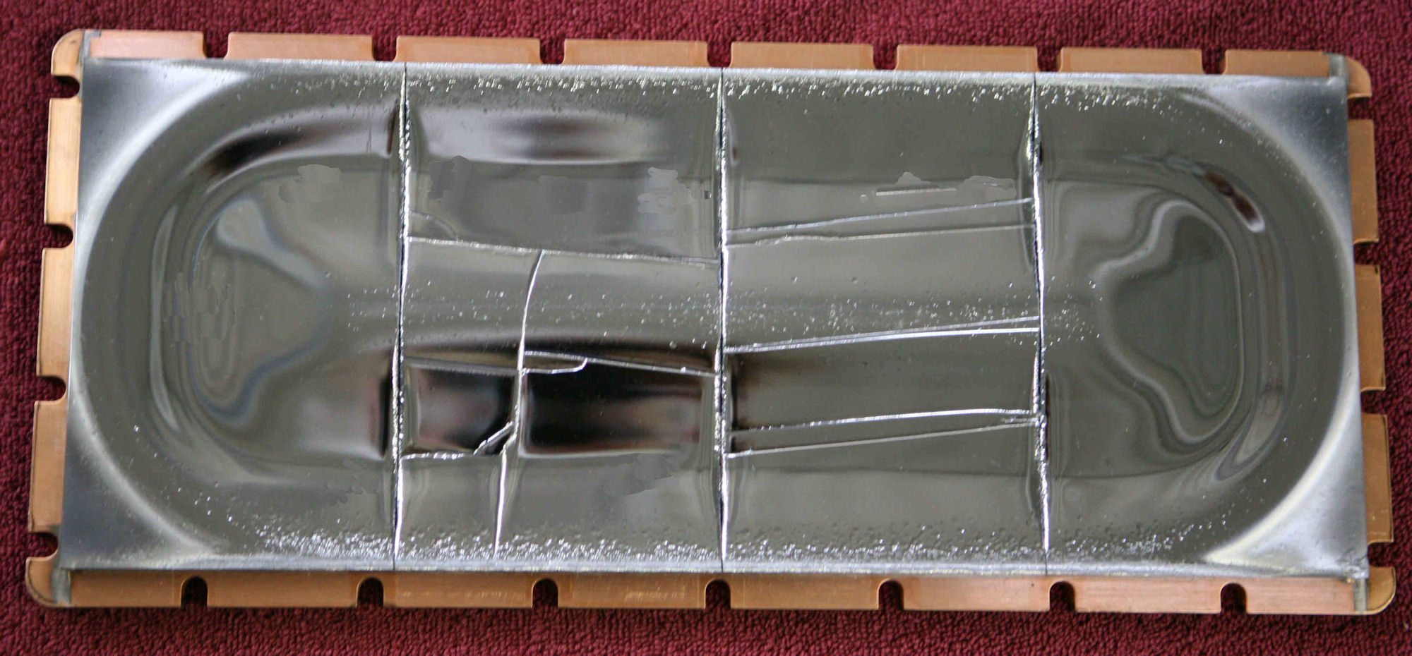
Q. Targets Crack
A. Possible causes: 
- Excessive thermal coefficient of expansion mis-match between target material and backing plate material as illustrated by the fractured doped Si target
bonded to a copper backing plate shown . This material, and most brittle and dielectric materials should be bonded to molybdenum target backing plates. - Backing plate is too thin and warps (“potato chips”), cracking the target bonded to it.
- Cooling water pressure exceeds recommended limit.
- Insufficient cooling water flow.
- Brittle materials should never be clamped to avoid fracturing the target.
- Targets fabricated from dielectric materials should not exceed 10” in length to prevent excessive thermal expansion, leading to cracking and potential
delamination from the backing plate. It is recommended that the overall target length be divided into a number of equal length tiles for these materials.
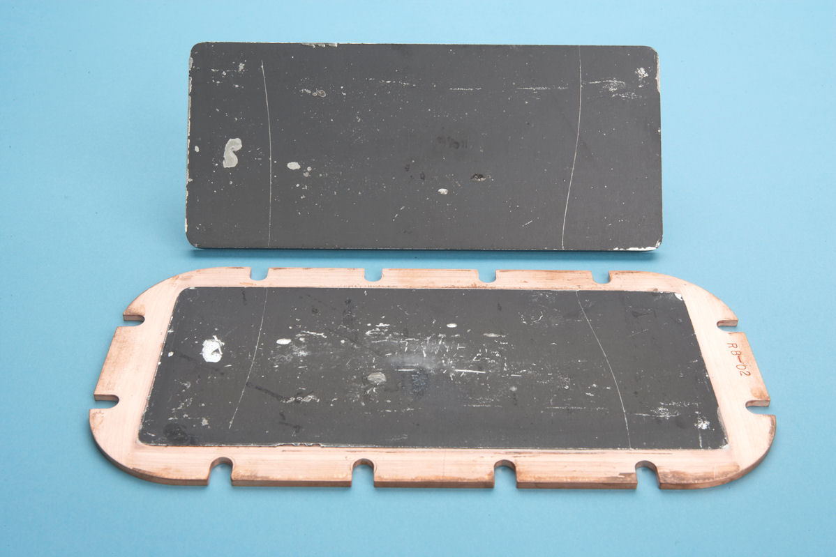
Q. Targets Debond from Backing Plate
A. Possible causes:  
Structurally strong target debonded from backing plate - Backing plate is too thin for the material it is made out of and does not have sufficient mechanical strength to withstand the typical nominal 70 psig force
(or greater) acting to deflect it. The backing plate warps to the point where the bond fails and the target is ripped from the backing plate (in the case of
structurally strong targets) or the target cracks and fractures (brittle and dielectric targets). Do not use copper when molybdenum is specified. - The entire bonding region must be completely filled with solder or elastomer. Significant voids (greater than 0.010” diameter) are unacceptable and should
be completely eliminated whenever possible as they lead to hot spots, spitting and melting of the solder or elastomer bond causing partial or complete target
delamination due to poor thermal transfer between the target and backing plate. Even if all voids are less than the maximum specified, the issues noted
above may still occur. It’s best to make certain that the entire bond is void-free. - Metallic solder bonding, using indium (minimum 90%) or silver alloys or elastomer bonding is preferred. Often it is necessary to deposit adhesion layers on
the target and backing plate bonding surfaces prior to making the solder bond. Good adhesion of this layer is critical to achieving a good bond. Failure to
follow this procedure will cause the target to debond. - There must be no voids in the solder edge at the target/backing plate interface. This junction must be smooth, continuous and completely filled with solder,
otherwise poor cooling may cause the bonding medium to melt and the failure to propagate. - Copper backing plates can anneal and lose structural strength after multiple target bonding/debondings, allowing the backing plate to warp and break the
bond. - Each time a copper backing plate is re-used, it usually must be resurfaced prior to bonding making it slightly thinner (thus less strong) each time. Replace
the backing plate with a new one. Since molybdenum is a refractory material, backing plates made from it are far less likely to be subject to this issue and
will last much longer.
|